Can India become the world’s BPO for semiconductors?
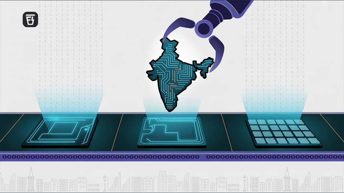
In today’s Finshots, we look at why India’s best shot at breaking into the semiconductor big league might be in chip packaging and testing, not building billion-dollar fabs.
But before we begin, if you’re someone who loves to keep tabs on what’s happening in the world of business and finance, then hit subscribe if you haven’t already. If you’re already a subscriber or you’re reading this on the app, you can just go ahead and read the story.
The Story
There has been a lot of buzz around semiconductor manufacturing lately. And it’s not hard to see why. Everything from your car, washing machine, and even your blood glucose monitor function only because of it.
Right now, the race to make those chips is turning into one of the most expensive and high-stakes games in the world. But chipmaking isn’t just about churning out silicon in shiny factories. It has anywhere between 400 to 1,400 processes!, which can be classified into three broad categories.
Act one is design: The blueprints, where engineers decide what the chip will do, how fast it will run, which processor architecture it uses (RISC or CISC), among other factors.
Act two is manufacturing: Billion-dollar semiconductor manufacturing facilities or what’s called as “fabs” carve microscopic circuits onto wafers using lithography, ion implantation, chemical processing, and millions of liters of ultra-pure water.
Act three is OSAT or Outsourced Semiconductor Assembly and Testing: This is where the backstage crew takes finished wafers, carves them into chips, wire-bonds them, tests them, and finally, packages them for shipping.
The real star of the show is, however, the second step. This is why everyone’s talking about building fabs. In fact, the Indian government has doled out incentives worth $10 billion just to get companies to invest in building fabs in the country.
But here’s the thing. India is not the only country to have these incentives. China and the US also have similar incentives worth over $50 billion. And we see the appeal.
A single fab can create thousands of direct & indirect jobs, and anchor an entire local ecosystem, attracting suppliers of chemicals, specialty gases, and precision equipment, as well as R&D labs and universities. And once a fab is up and running, it’s not easy to move. The sheer scale of investment, the need for a highly trained workforce, and the complex supplier network mean that the economic benefits tend to stick around for decades.
For governments, fabs are also about geopolitical autonomy. Having domestic fabs means fewer disruptions when geopolitical tensions flare up, and less dependence on imports for critical industries like defense, telecom, and healthcare.
However, at the same time, fabs are also high-tech, capital-intensive investments that can take years to build. And even after building them, the process of getting them to “full capacity” by calibrating equipment, fine-tuning yields, and ensuring you have the least defects can take another few years.
And that’s assuming you already have the right engineers, technicians, and supply chain partners in place. In reality, the talent pool for semiconductor manufacturing is small and highly competitive. Countries with established ecosystems, such as Taiwan and South Korea, have spent decades developing their expertise. For newcomers like India, even with generous subsidies, catching up means overcoming steep learning curves in both technology and human capital.
This is why, while fabs garner headlines, the real opportunity for India lies in the third step: Outsourced Semiconductor Assembly and Testing, or OSAT in short.
You see, OSATs need talent and low-cost labour. And that’s exactly where India already has a head start. We’re not starting from scratch. Bengaluru and a few other hubs already have a base in chip design, thanks to decades of work by global semiconductor giants running captive design centres here.
And India’s immediate strengths fit OSAT for a few reasons.
First, we have a large pool of electronics and software talent, strong handset and automotive supply chains, and improving logistics networks. Global semiconductor makers are also looking for more advanced packaging capacity after years of bottlenecks in the backend process. This means the demand is already there. We just have to position ourselves as a credible and scalable option.
Then, there’s a strategic advantage to starting here. Companies can build expertise in the latter end of the supply chain first, and only then move towards manufacturing wafers and designing them.
That’s because building and running a fab isn’t just about money, but also reliable electricity and water supply. Utilities must meet stringent 24/7 process specifications, and the current dependence on imports for tools and substrates can slow down production ramps. Plus, in a country grappling with periodic water shortages, building a plant that consumes millions of litres of ultrapure water isn’t exactly the most sensible starting point.
But this doesn’t mean that building OSATs first isn’t without problems.
The global competition is strong, and basic wire-bonding work won’t cut it if India wants to be taken seriously. We’ll need to move quickly into higher-value segments such as wafer-level packaging, fan-out technology, and heterogeneous integration. That in turn will require airtight IP protection, a predictable and stable policy environment, and customers who are willing to place long-term contracts.
The good news is that India already has multiple anchor projects in motion. Micron’s ATMP facility, HCL-Foxconn’s venture, and Tata Semiconductor facility are all in the works. On top of that, the government’s 50% capex grant significantly lowers the risk for early movers. The real challenge now is execution and delivering at a scale and quality level that matches established OSAT hubs like Taiwan, Malaysia, and the United States.
So, if we get the basics right, the upside is genuinely big.
When a car company wants to qualify a new power module with better thermal performance, it needs a shop that understands how to mount and cool it in a small space. When a server supplier wants chiplets stitched together inside a single package, it needs an integrator that can run that recipe day after day without hiccups. And these are not moonshots. India can keep those promises if we build the right machines, train the right people, and run the right playbook.
So, yeah. The bottom line is India can become a global hub for chip packaging even before it produces wafers competitively. The strategy should be to use generous OSAT incentives to lock in marquee customers, build vendor ecosystems for substrates and test handlers around existing plants, and upgrade local talent through joint programs with global toolmakers. Do this right, and India becomes indispensable to the world’s chipmakers.
That said, we can’t ignore the need to build competitive fabs, too. And that’s not just for economic value, but for resilience, as well as national security.
Until then…
Don’t forget to share this story on WhatsApp, LinkedIn and X.
Did you know? Nearly half of Indians are unaware of term insurance and its benefits.
Are you among them?
If yes, don’t wait until it’s too late.
Term insurance is one of the most affordable and smartest steps you can take for your family’s financial health. It ensures they do not face a financial burden if something happens to you.
Ditto’s IRDAI-Certified advisors can guide you to the right plan. Book a FREE 30-minute consultation and find what coverage suits your needs.
We promise: No spam, only honest advice!